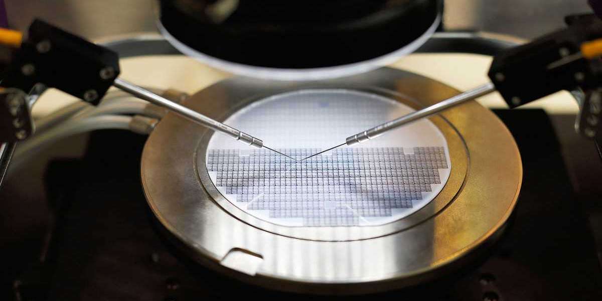
Getting the most out of your wafer reclaiming services will take some consideration, but with the right technology, you can achieve cost savings and increased efficiency. There are several process-specific and application-specific options available to you, but you'll have to weigh your options carefully before making a decision.
Technology advancements
Using reclaimed wafers in semiconductor applications can dramatically lower a chip maker's wafer cost. The cost of a 200-mm fab can be reduced by as much as one-fourth, according to the company. This has resulted in significant savings for major device manufacturers.
Silicon wafer reclaim services are available in many markets. Japan, France, and Germany are leading countries for reclaimed wafers. These nations are expected to see rapid growth in the next five years. Asia Pacific is also a region with high potential for market growth. In China, Korea, and Taiwan, the electronic industry is growing rapidly. The demand for consumer electronics is expected to surge, which will lead to a boost in the reclaimed wafers market.
The silicon wafer reclaim market is hampered by the complicated manufacturing process. The wafer is chemically cleaned, and then polished to restore the surface to prime levels. The surface is then dried and inspected with state-of-the-art metrology tools. The reclaimed silicon wafers can be used for a variety of applications, including solar panels and photovoltaic cells. For example, a reclaimed wafer can be used as a test wafer for high-voltage devices such as power circuits.
Cost savings
Integrated circuit manufacturers have found that silicon wafer reclaim is a viable cost-cutting strategy. This is because the technology has the ability to recycle refurbished wafers. Reclamation is a process that involves removing unwanted material from a wafer, grinding and polishing it to a grade A surface. The reclaimed wafers can then be reused in a variety of applications.
In the past few years, the semiconductor market has been sluggish. This has forced semiconductor manufacturing equipment developers to find new ways to lower costs. These developments have facilitated the growth of the reclaim market. The main application areas for silicon wafer reclaim are solar panels, optical devices, and other electronics. These markets are expected to experience significant growth over the next decade.
In addition to the solar industry, the demand for consumer electronics is expected to be a major driving force for the reclaim market. This is because the rising disposable incomes in conjunction with the growing population have led to an increased demand for electronics.
Processes involved
Currently, there are a variety of processes involved in wafer reclaiming services. These processes vary from simple strip and clean processes to complete repolishing. Each process has different specifications, and each service provider must meet the quality requirements of semiconductor device manufacturers.
Chemical etching is the most common technique used in conventional reclamation methods. During this process, chemicals are added to a tank to remove metal residues. This may result in stains from reaction products remaining on the back surface of the final product.
Reclaiming of used silicon wafers can provide significant cost savings for chip makers. Depending on the reclaiming method, metallic contamination levels can be reduced to as low as 30 microns. These wafers can be reused, extending the life of the wafer. Reclaimed wafers are typically thinner than fresh wafers, which provides an additional cost savings.
The reclaim process for silicon wafers is a multi-step process. The first step involves the inspection of the wafer surface. This is done using state-of-the-art metrology tools. The inspection results indicate whether the wafer is ready to undergo repolishing. During the repolishing, the wafer is chemically cleaned, inspected and rinsed. This is then followed by a series of finer polishing steps.
Segmentation by application
Among all the applications, solar cells are projected to dominate the silicon wafer reclaim market in the forecast period. It is expected to register the highest CAGR. The growth in the optoelectronic devices segment is also anticipated to be major. The 300mm segment is estimated to grow at a CAGR of 8.2% during the forecast period.
The global silicon wafer reclaim market is predicted to reach US$882 million by 2027. This is a substantial increase from the estimated value of US$529 million in the year of 2020. It is primarily driven by the rapid growth in demand for consumer electronics. Moreover, the increasing demand for low-cost consumer electronics and the shift toward renewable energy sources are likely to drive the silicon wafer reclaim market.
The development of the electronic industry in Asia Pacific is a key driving factor for the growth of the silicon wafer reclaim market. This region is characterized by the increasing adoption of renewable energy sources such as wind and solar power. The growing population in the Asia Pacific region has led to the surge in the demand for electronics. Moreover, the government has taken various initiatives to promote the development of the optoelectronics sector.


