Having a good understanding of probe card design is important, especially when you're developing a multi-DUT parallel test. In this article we will cover some of the challenges of designing a probe card. We'll also discuss some of the solutions available to you, including a FEA model of the probe card assembly.
FEA model for probe card assembly
Several important parameters were analyzed using a 3D simulation model in order to build a detailed probe card assembly model. These factors include fatigue life estimation, signal path optimization, and intermetallic contact quality. The results show how the different elements of the probe head impact its reliability.
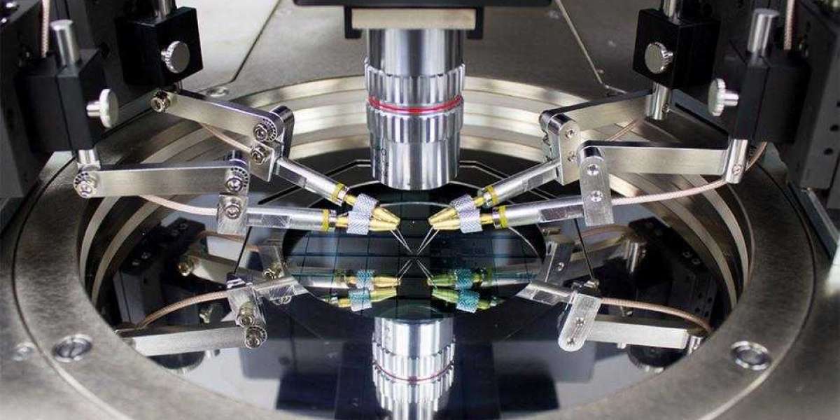
The probe head is a two-layer structure consisting of guiding plates and fillers between the plates. The guide plate is a ceramic material that was considered a rigid body. The ceramic was dyed a violet color to differentiate grooves from scratch marks.
The contactor carrier 20 is comprised of an intermediate plate carrier 26, a bottom plate carrier 28, and a top plate carrier 24. Each of these carriers has through holes to mount contactors 30. These carriers are mechanically and electrically connected to the probe card 260. The probe card ring is a robust piece of material that can withstand high temperatures. The contactor carrier is connected to the performance board 120 through cables 124. These cables transmit signals to the printed circuit boards 150. These printed circuit boards are also connected to the test head 100.
Problems with probe card design
Having a probe card fail prematurely can have a number of causes. It can be caused by process-induced defects, or it can be a result of a specific design problem. It's important to understand the probe-card design and manufacturing process in order to fully analyze a failure.
First, the contact resistance of the probes must be within specifications. If the contact resistance is too high, it can interfere with signals between the ATE and DUT. This can affect the ability to identify good dies and cause alarms on the test monitor.
Second, the thermal expansion coefficients of the probe card need to match those of silicon. Thermal expansion coefficients are critical because they can change the dimensions of the probe card as well as the temperature of the device. This can be an issue if the silicon wafer is heated to 150 * C. Third, the probes themselves are prone to wear. If the probe tips are worn, it can be an indication of a problem with the probe card design.
Solutions to multi-DUT parallel test
Adding parallel testing to your test system is an inexpensive and worthwhile addition, but there are several ways to go about it. For example, you can use multiple smaller power supplies, but this may not be the most cost-effective approach.
One solution is to connect several DUTs to a single SiteC. Then, you can configure the software to sequence test activities across DUT sites. The cost of this setup is likely to be a bit more than the initial cost of the power supply itself.
Another approach is to utilize a multi-site architecture, such as the Teradyne Magnum 2 test system. This architecture clones test programs into several sites, allowing you to perform device performance tests on all DUTs simultaneously. This type of setup is suitable for a wide variety of devices, including high speed DRAMs and logic devices. Lastly, you can employ traditional ATE parallel test techniques. This includes using a hardware module that supports features such as hardware state control and fast Fourier transform analyses.
Probe card operates well up to 3.1 Gbps
During semiconductor integrated circuits testing, a probe card is used to make contact with an IC wafer and to test it. It is a high-tech device that is used to test chips. A typical probe card has a number of parts that are made of different fragile materials. The primary components include the board and the probes.
The board acts as a support for the probe and ring assembly. It also provides the point where test signals from the probes are passed to the prober. The traces are thin strips of metal that are placed on the bottom of the board. The probes are then soldered to the traces. The metal pads are covered by a thin glass-like material called oxide. A camera is used in the prober to optically locate the probe card tips. This ensures that the probe makes an excellent electrical contact with the IC wafer. When a probe tip is contaminated, it affects the measurements of contact resistance.