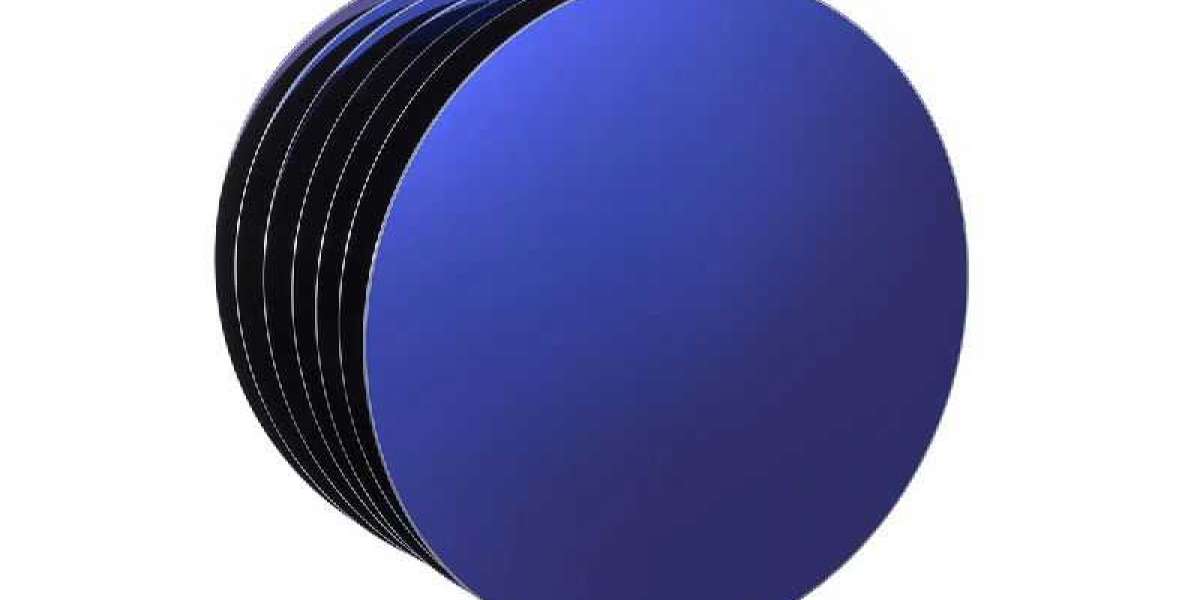
Silicon wafers are the future of the semiconductor industry. These 450-mm-long silicon wafers are the purest form of silicon ever made. Learn how they are made and how to clean them. You will also learn about float-zone silicon, the most pure form of silicon in existence. Here are some tips on how to clean a silicon wafer.
450-mm silicon wafers are the future of the semiconductor industry
The transition to 450-mm silicon wafers will have a number of implications for the semiconductor industry. First, it will alter supply chain dynamics, concentration of capital, and future RD capabilities. Second, it will alter the way that manufacturing takes place. This transition will involve significant changes in both processes and equipment, as well as the composition of the semiconductor industry.
Currently, processors and memory are made on 300-mm silicon wafers, which are about twelve inches across. The industry is moving towards 450-mm wafers to further reduce the costs of foundry operations and improve yields. Intel has led the way with this change. At present, 23 firms are operating 300mm fabs, and another 58 are still using 200mm wafers. Initially, 450-mm wafers were supposed to extend those cost savings even further, but high costs and uncertain rollout seem to have been a deterrent.
The cost of a 450-mm fab is about $10 billion to $15 billion. This is much more than the cost of a 200-mm fab. Moreover, the 450-mm fabs will also compete with 300-mm fabs, which are comparatively cheaper.
The transition to 450-mm silicon wafers will require an industry-wide shift. As a result, chip suppliers will be required to invest in new lithography tools. These new tools are being developed jointly and are expected to be available as early as 2009. These new lithography tools are an important step in the semiconductor industry's sustainability, as it will help companies increase their profits.
Float-zone silicon is the purest form of silicon ever created
The float zone silicon market is divided by node size, wafer bonding technology, end-user, and geography. The segmentation helps to identify core applications for float zone silicon. The report also offers insights on the competitive landscape. Geographically, North America is the largest market for float-zone silicon. Asia-Pacific is expected to grow at a rapid rate.
Float-zone silicon is less expensive than n-type silicon and can be produced more easily. However, to achieve high-resistance p-type silicon, polysilicon with low boron content is required. It can be further enhanced by adding small amounts of dopants via a process called pill doping. This involves drilling holes in the silicon ingot and evaporating the dopant layer onto the entire ingot.
Float-zone silicon is used in high-efficiency solar panels and other power devices. It is also highly transparent to terahertz radiation and is often used to fabricate optical components. But float-zone silicon is expensive. But new technology promises to slice a large ingot of float-zone silicon into thin wafers as small as three microns, thereby reducing costs and eliminating material loss.
The float zone method was invented by Henry Theuerer in 1955. This method produces the purest form of silicon ever created. It has a low concentration of impurities, typically less than five x 1015 cm-3. The silicon is grown in a vacuum or inert gaseous atmosphere with a monocrystalline seed crystal. A radio frequency field is then applied to melt the polycrystalline rod, thereby making contact with the monocrystalline seed crystal. The monocrystalline seed is then necked to form a high-purity monocrystalline crystal.
Cleaning a silicon wafer
Cleaning silicon wafer requires a combination of steps. The first step involves loading the silicon wafer into the pocket of an open-sided paddle with a handle that spins it inside a beaker filled with cleaning solution. The paddle is inert, so it will not react with the cleaning solution. The next step involves applying a chemical solution to the wafer to remove the particles.
The cleaning process begins by adding hydrochloric acid and deionized water in a weight ratio of 1:50. This step is done at 20deg C for five minutes. Once the cleaning step is complete, the silicon wafer is stabilized by forming an oxide film that prevents external contaminants from attaching and forming time-dependent haze. The cleaning process may also include the use of ultrasonic vibration to improve the cleaning performance.
Another method of cleaning a silicon wafer involves intentionally exposing the silicon wafer to a volatile solvent with a polarity between 2 and four. During the process, the volatile solvent removes the particles on the silicon wafer and prevents them from entering the source/drain extension region.
After the cleaning process is completed, the silicon wafer surface is rinsed with deionized water or ozone water. Then, the silicon wafer is dried (S27). Cleaning a silicon wafer with SC-1 and SC-2 cleaning solutions is a typical RCA procedure.